INGOAMPT AI News — Friday, 6 November 2026 · Europe/Vienna (CET, UTC+1). This is an original developer-focused explanation of new Reuters reporting published on 6 November. It is not a claim that all the underlying factory investments were announced today.
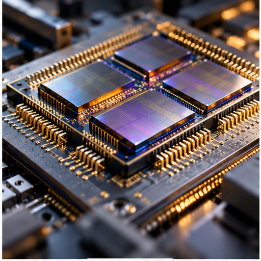
The race to build AI infrastructure is running into a less visible constraint: advanced semiconductor packaging. Reuters reported 6 November that makers of AI processors are investing heavily in techniques that bring different pieces of silicon—processors, memory and connections—close enough to exchange data at high speed.
Why packaging is important for AI
AI training and inference move substantial data between compute and memory. A fast arithmetic unit may be held back by how quickly data can move to and from its neighbouring components. Advanced packaging tackles part of this problem by physically connecting multiple chiplets through a shared structure. This is different from the familiar box around a consumer processor.
What Reuters verified
According to Reuters, TSMC dominates sophisticated chip-on-wafer-on-substrate (CoWoS) packaging, but tight capacity is motivating alternatives. The report cites research firm Yole Group’s forecast that 2026 capital expenditure on advanced packaging could approach $28 billion. It also covers Powertech’s planned $400 million venture with Broadcom in Singapore, with production targeted for 2028. Forecasts and prospective projects should not be mistaken for capacity already operating today.
Reuters further reported, based on an unnamed industry executive, that Nvidia is helping finance packaging capacity at ASE Technology’s SPIL subsidiary. Nvidia did not answer Reuters’ request for comment and ASE declined to comment on customer rumours. That sourcing limitation matters: we describe it as reported, not independently confirmed by the companies.
How a solo AI developer can use this information
- Separate hardware innovation from API availability. More packaging factories do not immediately translate to cheaper inference.
- Track latency and throughput. For an AI SaaS, model quality matters together with time-to-result and successful completion cost.
- Build geographic resilience. Services in the USA, EU and China may face different hardware access, terms and data rules.
- Avoid speculative projections. Do not market promised future performance as a current supported feature.
A learning exercise: chiplets, memory and bottlenecks
Draw an AI request as a pipeline: input tokens → memory access → computation → output → application response. Estimate which components contribute most to cost and latency in your actual workload. The packaging story matters because improving data movement can change infrastructure economics, but only benchmarks on the products you use can confirm the benefit.
Source and editorial method
Reuters, 6 November 2026: AI boom turns chip packaging into the next battleground. Figures and reported corporate plans are attributed to Reuters and the cited research; the developer takeaway is original INGOAMPT analysis. No copied publisher image has been used.